INDUSTRY
Odisha set to house India’s first, advanced, 3D chip-packaging unit
- IBJ Bureau
- Apr 20, 2026
A foundation stone for the country’s first, advanced, 3D chip-packaging unit has been laid at Info Valley in Bhubaneswar, Odisha.
The project marks a significant step towards strengthening India’s domestic semiconductor ecosystem and advancing the vision of Atmanirbhar Bharat in high-end electronics manufacturing.
A US-based technology firm, 3D Glass Solutions, is executing the project through its wholly-owned Indian subsidiary, Heterogeneous Integration Packaging Solutions.
Union Minister for Electronics & IT Ashwini Vaishnaw has said that the foundation stone of a semiconductor plant has been laid in Odisha on the occasion of Akshay Tritiya. He has added that the upcoming facility marks a significant step for high-tech manufacturing in the State.
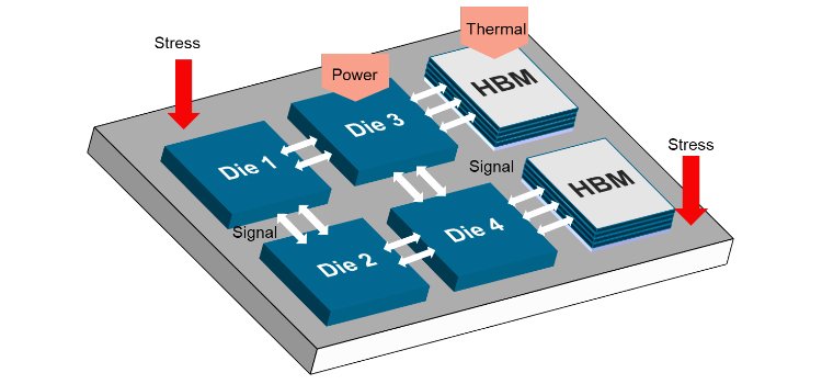
Calling it a matter of pride for Odisha, the Union minister has said that the plant will be based on advanced technology, including the use of 3D glass substrate technology in chip manufacturing. He described this as a next-generation innovation in the semiconductor sector.
Addressing the gathering, Odisha Chief Minister Mohan Charan Majhi has described the project as a historic milestone for Odisha and the nation. He said that for the first time in India, an advanced 3D glass solutions semiconductor project is being established, bringing immense pride to the State.
He has also noted that global technology leaders such as Intel, Lockheed Martin and Applied Materials are associated with cutting-edge packaging technologies, and their interest in Odisha reflects the State’s growing industrial strength.
Mr Majhi has said that the company is investing nearly Rs 2,000 crore in the project, and the facility is expected to produce 70,000 glass panels annually, along with 5crore assembled units and around 13,000 advanced 3DHI modules.


Report By
View Reporter News